Michelle Li and Jinrong Qian, Texas Instruments
End-user demand for fast and efficient charging is continuous and ever-growing. The Lithium-Ion (Li-Ion) battery is desirable because it has very high energy density. These batteries have a high-charge current that works well for 10-inch tablet applications and a high battery pack capacity of more than 6 Ah. Tablets require superior thermal performance and instant turn-on, even with a deeply discharged battery. These requirements present a few technical challenges. First, how to maximize available power from power sources to efficiently and quickly charge the battery while not crashing the power source. Second, how to charge a deeply discharged battery while operating the system simultaneously. Lastly, how to improve thermal performance.
Dynamic Power Path Management
How to maximize available power to charge the battery quickly and efficiently? Every power source has its output current, or power limit. For example, the maximum output current is limited to 500 mA from a High-Speed USB (USB2.0) port, and up to 900 mA from a SuperSpeed USB (USB3.0) port. The power source will crash if the system power demand exceeds the power available from the power source. When charging the battery, how do we prevent a power source crash while maximizing the power output? Three control methods are introduced: input current-based dynamic power management (DPM), input voltage-based DPM and battery supplement mode.

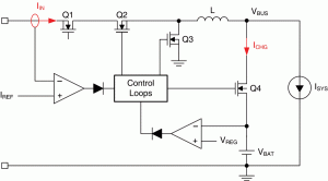
Figure 1 shows a high-efficiency switch-mode charger with DPM controls. MOSFETs Q2 and Q3 and inductor L are composed of a synchronous switching buck-based battery charger. This combination achieves the highest possible battery charging efficiency and fully uses the adapter power for achieving fastest charging. MOSFET Q1 is used as a battery reverse blocking MOSFET for preventing leakage from the battery to the input through the body diode of MOSFET Q2. It is also used as an input current sensing element to monitor the adapter current.
MOSFET Q4 is used to actively monitor and control the battery charging current to achieve DPM. When the input power is sufficient to support both system load and battery charging, the battery is charged with the desired charge current value of ICHG. If system load ISYS is suddenly increased and its total adapter current reaches the current limit setting IREF, the input current regulation loop actively regulates and maintains the input current at the pre-defined input reference current of IREF. This is achieved by reducing the charge current while giving higher priority of powering the system to reach its highest system performance. Therefore, the input power is always maximized without crashing the input power source, while the available power is dynamically shared between system and battery charging.

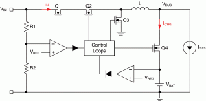
If a third party power source is plugged into a system that cannot identify its current limit, it is difficult to use the input current limit-based DPM. Instead, the input voltage-based DPM is used. Its control diagram is shown in Figure 2. Resistor divider R1 and R2 are used to sense the input voltage and are fed into the error amplifier of the input voltage regulation loop. Similarly, if the system load is increased, causing the input current to exceed the adapter current limit, the adapter voltage starts to decrease and eventually reaches the predefined minimum input voltage.
The input voltage regulation loop is activated to maintain the input voltage at the pre-defined voltage. This is achieved by automatically reducing the charge current so that the total current drawn from the input power source reaches its maximum value while not crashing the input power sources. Therefore, the system now can track the adapter’s maximum input current. The input regulation voltage is designed in such a way that its voltage is still high enough to fully charge the battery. For example, it can be set around 4.35 V to fully charge a single-cell, Li-Ion battery pack.
Both input current and input voltage-based DPM controls can draw the maximum power from the adapter and not crash the adapter. For portable devices such as smartphones and tablets, the system load is usually dynamic with a high pulsating current. What happens if the pulsating system peak power is higher than input power, even when the charge current is already reduced to zero? The input power source could crash without active control.
One solution is to increase the adapter power rating, but this increases the adapter’s size and cost. Another solution is to temporarily discharge the battery by supplementing the power to the system besides the available power from the adapter. So, the battery supplies additional power by turning the MOSFET Q4 on to discharge instead of being charged. By combining the DPM control and the battery supplement mode, the adapter can be optimized to support the average power, instead of the maximum peak system power for cost reduction and achieving smallest solution size.
Design Considerations for Improving System Performance

Portable power systems, such as tablets and smartphones, require an “instant on” capability to improve the user experience. This means that whether the battery is fully charged or deeply discharged, the system will turn on instantly when an adapter is plugged in.
Let’s re-exam the system in Figures 1 and 2 and use a one-cell Li-Ion battery system as an example. If the battery is directly connected to the system without MOSFET Q4, system bus voltage of VBUS is the same as battery voltage. For a deeply discharged battery with less than 3 V, its voltage is not high enough to turn on the system. The end users need to wait until the battery is charged to 3.4 V before turning on the system. In order to support system instant on, a MOSFET Q4 is added to operate in linear mode to maintain the minimum system operation voltage, while simultaneously charging a deeply discharged battery. The minimum system voltage is regulated by the switching converter, while the charge current is regulated by the LDO mode by controlling MOSFET Q4. Once the battery voltage reaches the minimum system operation voltage, the MOSFET Q4 is fully turned on. Its charge current is regulated by the duty cycle of the synchronous buck converter. So, the system voltage is always maintained between the minimum system operation voltage and maximum battery voltage for powering the system.

How to extend the battery run-time? Of course, the higher the battery capacity, longer is the battery run-time. For a single-cell operating system, the typical minimum system voltage is around 3.4 V in order to reach a 3.3 V output usually required by a system. If the on-resistance of MOSFET Q4 is 50 m?, and battery discharge current is 3 A, battery cut-off voltage is 3.55 V. This means that more than 15 percent of the battery capacity is unused and remains in the battery. In order to maximize the battery run-time, the on-resistance of MOSFET Q4 must be designed as small as possible, for instance 10 m?.
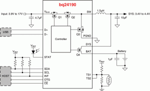
Figure 3 shows an example of a high-efficiency, single-cell I2C battery charger with integrated MOSFETs. This charger supports both USB and AC adapter inputs for tablet and portable media device applications. All four power MOSFETs are integrated, while MOSFETs Q1 and Q4 are used to sense the input current and battery charge current for further minimizing the system solution size. This charger can detect the power source between a USB and an adapter to quickly set up the correct input current limit.
Additionally, the charger also can charge the battery as a standalone charger with internal default charge current, charge voltage, safety timer and input current limits, even when the system is turned off. It also has a USB On-The-Go (OTG) function by operating the charger in boost-mode to provide 5 V/1.3 A output at the USB input from the battery.
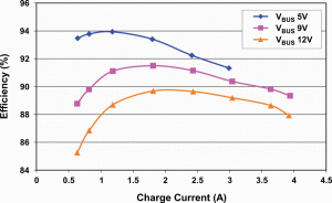
Thermal performance is critical for portable devices with a very thin surface because users easily could feel the heat coming from the PCB board. To combat this, optimized high efficiency and good layout design are very important. To further improve the thermal performance, a thermal regulation loop is introduced. It maintains the maximum junction temperature by reducing the charge current once it reaches the pre-defined junction temperature. Figure 4 shows the measured battery charge efficiency. Up to 94 percent efficiency can be achieved with 5 V USB input. It only has a 32°C temperature rise with 9 V input and 4 A charge current.
Summary
The dynamic power management with battery-supplement-mode is critical for optimizing the battery’s charge system performance. Both input current and input voltage-based DPM are used to power the system with instant-on while simultaneously charging the battery. Critical design considerations such as battery run-time and thermal performance are also discussed.
References
For more information about battery charge management, visit: www.ti.com/batterycharger-ca. Download a datasheet for the bq24190 here: www.ti.com/bq24190-ca.
Michelle Qiong Li is a systems engineering manager and manages the systems engineering team in TI’s Battery Charger Management group. This group is responsible for product definition, evaluation, roadmap and customer solutions for battery chargers in notebook, tablet, media device, medical and industrial portable equipment markets. Michelle received her Ph.D. from the Center for Power Electronics Systems (CPES), Blacksburg, Virginia. She holds 14 US patents.
Jinrong Qian is a product line manager of battery charge management and an Emeritus Distinguished Member of the TI’s Technical Staff for Battery Management Solutions. He has published a myriad of peer-reviewed power electronics transactions and power management papers, and holds 26 US patents. Dr. Qian earned a BSEE from Zhejiang University and a Ph.D. from Virginia Polytechnic Institute and State University.
If you have any questions about this article, please contact ti_jinrongqian@list.ti.com.
This article appeared in the March/April 2012 issue of Battery Power magazine.


